Capacitors
C1
47 uF 16V Electro
C2
47 uF 16V Electro
C3
2n2 Ceramic
C4
47 nF Polyester
C5
2n2 Ceramic
C6
2n2 Ceramic
C7
100n Polyester
Resistors -
all ¼ or ½ watt metal film
R1
100 ohm
R2
100 ohm
R3
10k
R4
470k
R5
1k
Semiconductors
Q1
BC549C
Misc.
SW
Ganged with PTT switch, on during Tx
Electret
2-wire electret microphone insert
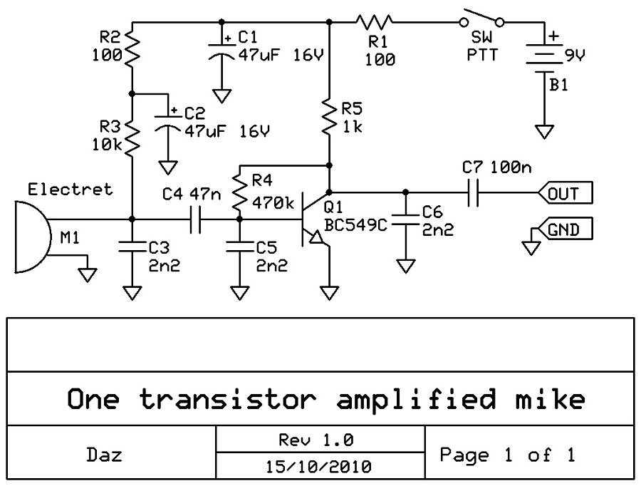
Q1 is used as a typical common-emitter small signal amplifier. Bias is applied via
R4 to keep the transistor biased near the midpoint. R5 is the output collector
load. R1 & C1 filter the supply voltage to reduce turn-on clicks, C2
decouples the supply voltage to the electret mike to prevent feedback via
the supply rail. A BC549C transistor is recommended for low noise, and
high gain. Gain depends on the individual transistor characteristics, and
can be from 15 to 25 dB. Current consumption is around 5 mA.
C3, C5 and C6 decouple the input and output from nearby RF. This prevents RF feedback from occurring. C3 needs to be placed directly at the rear of the microphone element. Connect the mike element using shielded cable to prevent hum pickup.
The coupling capacitors C4 and C7 have values chosen to reduce low frequency content in the audio below 300 Hz. The values can be changed if required, and aren't critical.
There is no
level control in this circuit. Use the transceiver mike gain control instead,
or add a 10k pot at the output terminals, wired as a voltage divider (normal
volume control).
Capacitors
C1
47 uF 16V Electro
C2
47 uF 16V Electro
C3
2n2 Ceramic
C4
100n Polyester
C5
2n2 Ceramic
C6
120n Polyester
C7
10n Polyester
C8
82n Polyester
C9
47n Polyester
C10
100n Polyester
C11
47n Polyester
C12
2n2 Ceramic
C13
1uF 16V Electro
Resistors -
all ¼ or ½ watt metal film
R1
100 ohm
R2
100 ohm
R3
10k
R4
470k
R5
1k
R6
20k
R7
20k
R8
10k
R9
1k
L1 47 mH choke inductor
Semiconductors
Q1
BC549C
Q1
BC549
Misc.
SW
Ganged with PTT switch, on during Tx
Electret
2-wire electret microphone insert
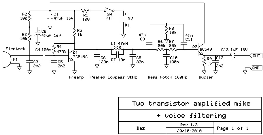
Q1 is used
as a typical common-emitter small signal amplifier. Bias is applied via
R4 to keep the transistor biased near the midpoint. R5 is the output collector
load. R1 & C1 filter the supply voltage to reduce turn-on clicks, C2
decouples the supply voltage to the electret mike to prevent feedback via
the supply rail. A BC549C transistor is recommended for low noise, and
high gain. Gain depends on the individual transistor characteristics, and
can be from 15 to 25 dB. Current consumption is around 9 ma.
C3, C5 and C6 decouple the input and output from nearby RF. This prevents RF feedback from occurring. C3 needs to be placed directly at the rear of the microphone element. Connect the mike element using shielded cable to prevent hum pickup.
The input coupling capacitor C4 reduces low frequency content in the audio below 300 Hz.
There is no level control in this circuit. Use the transceiver mike gain control instead, or add a 10k pot at the output terminals, wired as a voltage divider (normal volume control).
The output filter consists of two stages, a lowpass and a bass notch filter.
Lowpass:
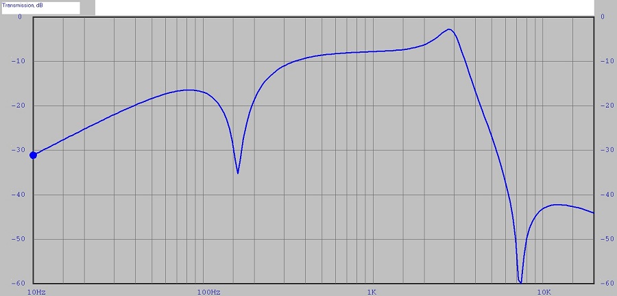
The lowpass
filter serves two purposes: It boosts the high frequency content by more
than 3 dB, and it sharply cuts frequencies over 3 kHz, which can cause
adjacent channel splatter on AM. It is implemented as a type of elliptic
filter, which consists of a lowpass filter with a notch added for a sharper
cutoff.
Bass notch
filter:
The bass notch
filter sharply reduces power-hungry low frequency energy around 100 to
200 Hz, without being overly complex.
* revised 20/10/2010 - Buffer amplifier added to output to make unit insensitive to transceiver input impedance
Frequency response
plot:
For reference: IC1 = NJM2902N = LM324 quad OpAmp equivalent
Part numbering is from Pearce Simpson Super Cheetah schematic
Procedure:
Remove R232 (4M7 squelch hysteresis)
Add 100k resistor from pin 8 to pin 9 on IC1 (linearization)
Add 100n monolithic capacitor from pin 8 to pin 9 on IC1 (smoothing)
Replace C28 22uF with 100n monolithic (faster smoothing)
Replace R40 3k3 with 100k (linearization)
Short out R314 (wire ccw
end of squelch control directly to GND) (squelch control range fix)
Add 47k from pin 9 on IC1
to pin 7 on IC1 (direct feed from AGC amp)
Optional: (improved muting response)
Replace TR11 with a VN10KM MOSFET (better linearity) - form leads to fit: D=C G=B
S=E
Replace R40 3k3 with 470k (better smoothing)
This makes the muting audio level control more linear.
All resistors Carbon or Metal Film 0.25 or 0.5 watt miniature
This conversion makes the Squelch control into a linear acting mute. Signals are unmuted proportionally
to their strength, with no delays. This allows weak signals to still be heard at low volume, and can effectively suppress noise in between words on SSB.
This mod changes the way the Squelch function mutes the audio, from simple on-off to a smooth one (variable attenuator). This makes SSB audio sound much cleaner, and can even suppress noise in between words or syllables.
A similar mod can be done on many different reciever and transciever types, including 27MHz CB radios. The example here applies to the FT-747 only.
Changes required:
1. A feedback RC network is connected to the Squelch amp Q14b pins 6 and 7, consisting of a 100k resistor in parallel with a 39n MKT polyester cap. This linearizes and smoothes the Squelch amplifier response. (Q14 is an 8 pin DIP OpAmp located under the "Local Unit" plug-in PCB.)
2. The 2nd muting transistor Q17 is removed from circuit. Either cut the base or collector lead, or desolder it and remove it. (Q17 is located near J26, the FM board connector.) If this transistor is not disabled, it results in distorted audio during partial muting.
3. The "Hang" AGC is disabled, by cutting or removing R75 from circuit (10k). This speeds up the AGC for better muting action. (R75 is located about 1 inch away from Q17, towards the "Local Unit" PCB.)
4. Cut D29. This prevents the S-Meter being turned off by the Squelch muting. (D29 is near J24)
5. OPTIONAL: Add a 100n polyester capacitor from the AGC line to ground to improve smoothing. This can be added anywhere on the AGC line (one easy location in from R33 near Q03 to the ground lead of C80).
6. OPTIONAL: Change C130 (4n7) to 2n7 to increase treble response of receiver.
7. Reconnect and turn on transciever. Set Squelch control to zero and adjust VR05 to restore fully unmuted audio.
TESTING: Tune in a moderately strong SSB signal, and turn the Squelch control up until the background noise disappears. Perceived quality dramatically improves. Best Squelch control position is between 9 o'clock and 12 o'clock depending on signal strength.
This mod does not affect FM mode very much, as the FM board has it's own muting circuit.
Future alterations for experimenters: Better noise suppression on strong signals could be obtained if the Squelch threshold could be automatically increased for strong signals. This could be achieved by a slow time constant filter fed from the AGC voltage that would offset the threshold in a positive direction. this would require buffering, smoothing and inversion of the AGC voltage levels.
This modification does not increase power, it only makes the modulator stage more rugged, and able to handle higher current demands!
If your radio is working well already, there is nothing to gain from this mod.
If you have had repeated 2SA1012 failures, or are having trouble finding a genuine 2SA1012, this mod is for you!
Disconnect the power to the radio first, as the modulator stage is permanently connected to the 13.8V line!
Remove 2SA1012 bipolar transistor - keep all mounting hardware
Replace 2SA1012 with an IRF4905* or IRF9540 P-channel MOSFET - Carefully clean off mica washer and heatsink surface, then apply new thermal paste and mount MOSFET normally & solder in
Remove TR43 (2SB525) - it is not required
Move R213 (10k) to connect from MOSFET gate to MOSFET source terminals
Add a wire link from MOSFET
gate to TR42 (2SC945) collector
Replace R215 (150 ohms 1/2W) with a wire link (ie: short it out)
Add a 220 ohm 1/4W resistor from TR42 emitter to GND
Power up, and using a 50 ohm dummy load, readjust AM
POWER for 4 watts average carrier power on AM transmit when unmodulated.
Using a 1kHz sinewave tone, test that AM modulation reaches close to 100% with no major distortion.
(use a CRO, or check that no adjacent channel splatter is present)
At 4W average AM carrier power, 100% modulation should be hitting around 16W PEP (typically higher)
Test that close to 13.8V is present on the MOSFET drain terminal in SSB transmit mode
2SA1012 ratings: 5A, 25W, <0.4V Vsat
IRF9540 ratings: 23A,
130W, on resistance = 0.117 ohms
IRF4905 ratings: 74A,
200W, on resistance = 0.02 ohms *preferred choice
Therefore, a P-Channel power MOSFET should be much more rugged than the 2SA1012, and drop minimal voltage in SSB mode.
Part numbering from Super Cheetah schematic:
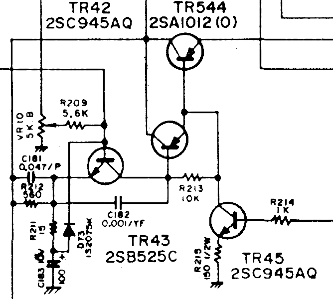
TR42 amplifies the audio from the microphone amplifier stages, and drives darlington pair TR43 and TR544. Since both the TR42 and TR43/TR544 stages are common emitter, the signal is amplified and inverted twice. Some negative feedback is applied via R212 back to TR42's emitter. This helps reduce distortion and stabilize the DC operating point (AM carrier power).
C183 is originally a 10V rated part, but is subject to over 12V in SSB mode. It should be replaced with a 16V 100uF electro.
A PNP power transistor is used for TR544 to pass the heavy current to the final and driver stages
with minimal voltage drop. Low voltage drop is important for maximum peak
power capability. This is the reason behind using the 2SA1012, with it's
very low Vsat voltage of <0.4V.
Modified circuit:
This mod was first tested with an IRF9540, but an IRF4905 works better due to lower on-resistance.
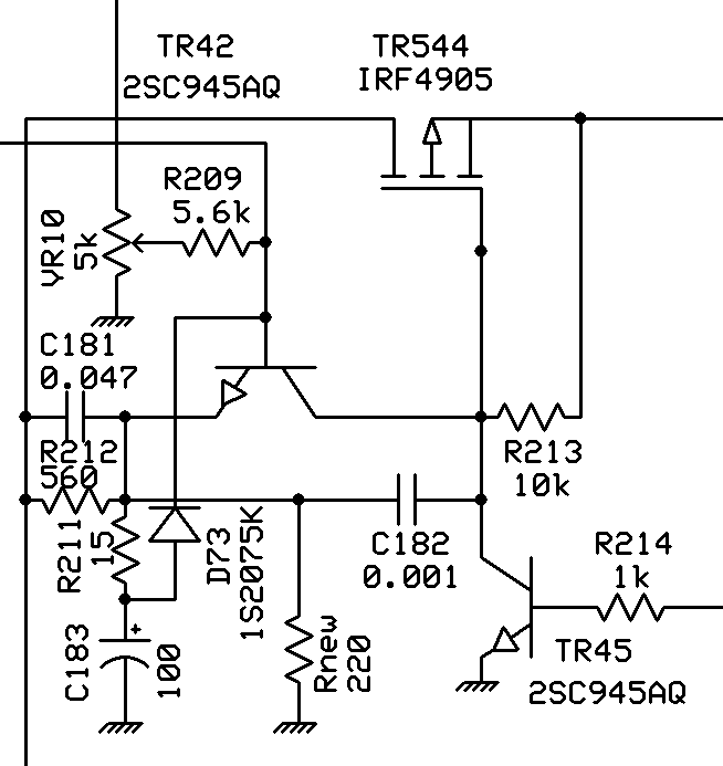
The modified circuit has TR43 removed, and the TR42 collector connected directly to the MOSFET gate.
R215 is replaced with a short, because MOSFETs are voltage controlled, not current controlled. This means in SSB mode TR45 can switch the MOSFET gate to ground, placing almost the full 13.8V across the MOSFET gate/source junction. This is more than enough to turn TR544 fully on for lowest on resistance, thus allowing the RF final and driver stages to get as close as possible to the full 13.8 volt supply.
Rnew is required to pull TR42's emitter closer to ground so the MOSFET can get sufficient gate drive to turn fully on during positive AM modulation peaks. Unfortunately, this makes the DC operating point of the circuit less stable, and the AM power adjustment more critical.
The distortion performance of this circuit may be inferior to the original configuration for two reasons:
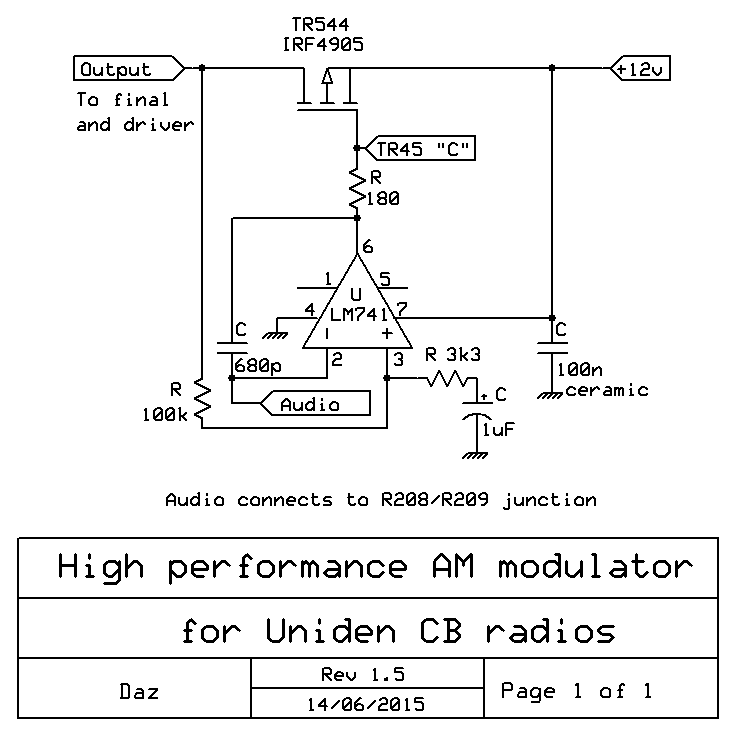
The P-channel MOSFET functions as a common source inverting amplifier, so the negative feedback goes via a 100k resistor to the non-inverting OpAmp terminal. The 3k3 resistor scales the negative feedback to set the gain. The negative feedback helps linearize the MOSFET for low distortion. The 1uF capacitor degenerates the total gain at DC to produce a stable operating point (carrier power). Because there is no feedback resistor from the OpAmp inverting terminal to the output terminal, the entire OpAmp open loop gain is available at DC to correct for the MOSFET linearity and temperature drift characteristics.
The 100n ceramic capacitor decouples the supply rail at high frequencies to assist stability. The 680p capacitor produces a dominant pole to help stabilize the negative feedback by reducing the gain at frequencies where the system would otherwise be unstable due to phase shifts caused by MOSFET gate capacitance.
MOSFET final and driver
conversions done properly
IRF540 - Applying correct bias and thermal bias compensation, tuning